 |
| Universal dispersion model
Universal dispersion model (UDM) is basic model used in newAD2 for calculation of
optical constants of condensed matter [7,8]. Model have no constant number of parameters.
Number of the parameters depends on how many terms model contains. Individual terms represent
types of elementary excitations in condensed matter. Number of terms is modified by model attributes
and model contains at least three parametric contribution representing interband electronic transitions.
The attributes and values of parameters can be saved to the file
Universal-id.par in the command line mode of newAD2 by:
par save.
This is way how to distribute optical constants between individual fits of users.
In the model (in modelfile) the name of parfile
can be introduced instead of attributes:
modelfile
Universal[:attributes|parfile]
parfile
attributes
Nvc = value
Eg = value
Eh = value
...
newAD2 command
parameters save Universal-id(save attributes and parameter values of medium id in the Universal-id.par)
Note that attributes and parameters are order insensitive.
udm program
The results of optical characterizations based on UDM can be easily exported by simple program udm. This utility generate table of optical constants as function of photon energy (eV), wavelength (nm), wavenumber (1/cm) or frequency (THz).
Usage:
udm
- display help
udm parfile
- print table of optical constants of material defined in parfile
(4001 lines for energy in range 0.01-100 eV with exponential distribution)
udm parfile lambda=190~850:661
- print table of optical constants of material defined in parfile
(661 lines for wavelength in range 190-850 nm withe linear distribution, i.e. with step 1 nm).
Fore more see help.
Download:
source code in C++
for Linux
for Windows
Electron excitations
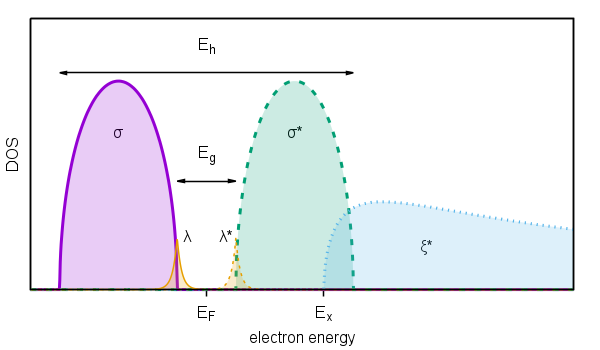
Figure 1. Schematic diagram of density of states (DOS) of valence electrons electrons:
σ - valence band;
σ* - conduction band;
ξ* - band of higher excited states;
λ - occupied localized states;
λ* - unoccupied localized states.
Using of individual attributes corresponding to the individual types of elementary excitations will be demonstrated in the following sections. For description of electronic excitations the basic schema introduced in Fig. 1 will be used. Therefore, electronic excitations can be classified by all possible combinations of transitions between occupied bands σ and λ end empty bands σ*, λ* and ξ*.
Interband transitions
Basic three-parametric model includes electronic transitions from valence to conduction bands.
In the basic schema this transitions are represented by σ → σ*.
The parameters of this model are

Figure 2. Schematic diagram of joint density of states of interband transitions.
modelfile
Universal
parfile
Nvc = 400
Eg = 5
Eh = 30
Note that in this case the parfile begin by obligatory empty line.
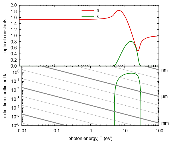
Figure 3. Optical constants calculated on the basis of three-parametric
dispersion model of interband transitions. The gray lines represents absorption thresholds
for given thickness of ambient.
Dielectric response exhibit nonzero absorption only for photon energy in the range from
Modification of interband transitions by excitons
In the condensed matter the redistribution of transition strength from higher energies to the spectral parts with lower energies is presented
due to multi-particle effects. Therefore, course of absorption is is deformed in comparison to the course of absorption corresponding to the
one-particle approximation. Especially, for sufficiently low temperatures the crystalline matter exhibits sharp
structures generally called excitons which disappear for high temperatures. Simultaneously joint density of states can exhibits also relatively
sharp structures called Van Hove singularities, however temperature practically independent. Finally, the absorption bands of condensed
matter exhibit various form given by forms of density of states (DOS) of valence and conduction electrons and probabilities of transitions
of electrons between these occupied and unoccupied bands. All these effect even though they are or they are not true excitons are modeled by
`excitonic' contributions described by 3 parameters:
As a example the modification with two excitons will be introduced even when the number of excitons is unlimited.
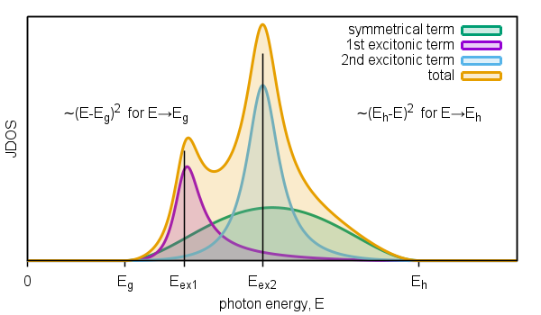
Figure 4. Schematic diagram of joint density of states of interband transitions modified by two excitons.
modelfile
Universal:ex=2
parfile
ex=2
Nvc = 400
Eg = 5
Eh = 30
A0 = 1
Aex1 = 0.2
Eex1 = 6
Bex1 = 0.5
Aex2 = 0.3
Eex2 = 12
Bex2 = 1
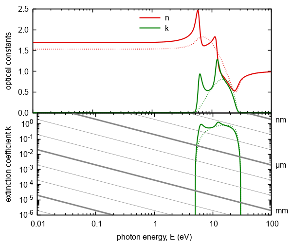
Figure 5. Optical constants of the interband transitions modified by two excitonic terms. Doted lines represent
model without excitonic modification. The gray lines represents absorption thresholds
for given thickness of ambient.
Note that negative or invalid value of attribute
Excitations of valence electrons into the higher energy states
In addition to excitation of valence electrons into the conduction band the electrons can also be excited into the higher energy states.
As excited electron energy is higher as the final states losing band character and electrons are closer to free electrons,
i.e. described by endless band without significant structures. Therefore, joint density of states approach to zero as
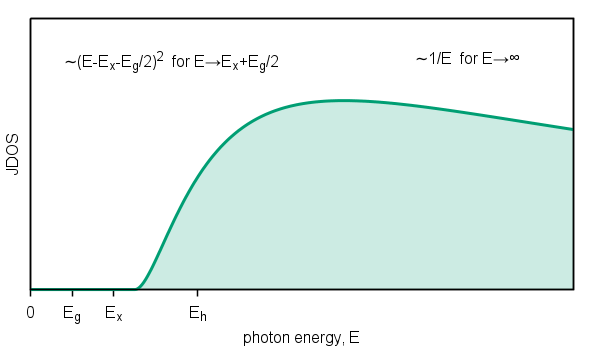
Figure 6. Schematic diagram of joint density of states of transitions into the higher energy states.
modelfile
Universal:ex=2:he
parfile
ex=2:he
Nvc = 400
Eg = 5
Eh = 30
A0 = 1
Aex1 = 0.2
Eex1 = 6
Bex1 = 0.5
Aex2 = 0.3
Eex2 = 12
Bex2 = 1
Nvx = 1000
Ex = 10
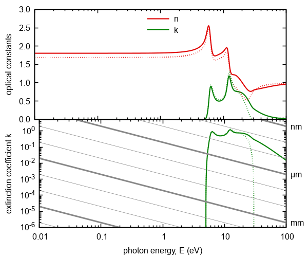
Figure 7. Optical constants calculated on the basis of model of excitations of extended valence electrons.
Doted lines represent model without transitions into higher energy states. The gray lines represents absorption thresholds
for given thickness of ambient.
We note that absorption of this contribution begins at energy
Urbach (exponential) tail
When characterizing films in a spectral range around band gap energy
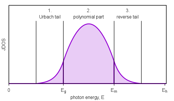
Figure 8. Schematic diagram of joint density of states representing Urbach (exponential) tail.
modelfile
Universal:ex=2:he:ut
parfile
ex=2:he:ut
Nvc = 400
Eg = 5
Eh = 30
A0 = 1
Aex1 = 0.2
Eex1 = 6
Bex1 = 0.5
Aex2 = 0.3
Eex2 = 12
Bex2 = 1
Nvx = 1000
Ex = 10
Nut = 40
Eu = 0.1
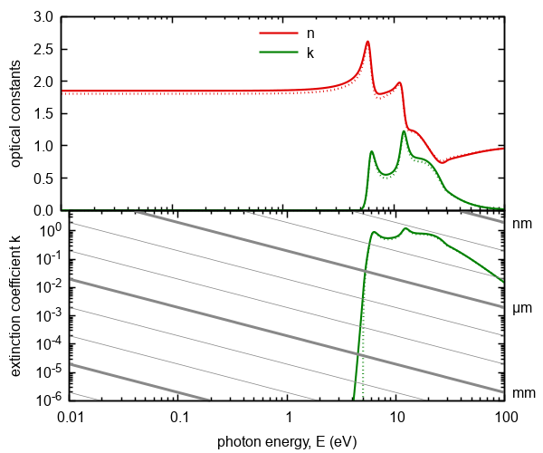
Figure 9. Optical constants calculated on the basis of the model included excitations from/into localized into/from extended states
(Urbach tail). Doted lines represent model without localized states contributions. The gray lines represents absorption thresholds
for given thickness of ambient.
We note that the usage of "Urbach tail" name should be restricted only to describe effects caused by localized states originated in disorder of amorphous materials. The typical value of Urbach energy at the room temperature is about 50 meV. The term "exponential tail" is more suitable in other cases. The origin of join density of states as used in UDM is given by the assumption of symmetry of valence and conduction band. However, there is actually no reason for this assumption, hence the model should in theory contain at least two Urbach energies corresponding to λ → σ* and σ → λ* absorption processes. Moreover, localized states have different origins and should have also different characteristic energies and transition strengths. In reality they are indistinguishable and according to our experience the two parameter model is sufficient.
Absorption of the localized states
The last electron excitations type missing in UDM are transitions between localized electron states represented in the basic schema as λ → λ* transitions. They can be easily modeled by Gaussian-broadened discrete spectra (Gaussian peaks), where every characteristic energy corresponds to single type of localized states. This is not the case for broad absorption peaks which can not be connected to such processes (in this case they represent rather λ → σ* a σ → λ* transitions described in the previous paragraph). Each absorption peak in the model is characterized by three parameters:
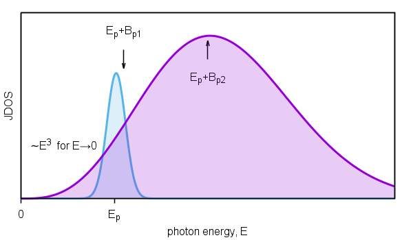
Figure 10. Schematic diagram of joint density of states of Gaussian broadened peaks. In the figure are introduced two extreme
examples, i.e. when broadening energy is comparable or higher then characteristic energy and example when broadening energy is much
smaller than characteristic energy.
modelfile
Universal:ex=2:he:ut:loc=2
parfile
ex=2:he:ut:loc=2
Nvc = 400
Eg = 5
Eh = 30
A0 = 1
Aex1 = 0.2
Eex1 = 6
Bex1 = 0.5
Aex2 = 0.3
Eex2 = 12
Bex2 = 1
Nvx = 1000
Ex = 10
Nut = 40
Eu = 0.1
Nloc1 = 0.1
Eloc1 = 4.5
Bloc1 = 0.5
Nloc2 = 0.001
Eloc2 = 3
Bloc2 = 0.1
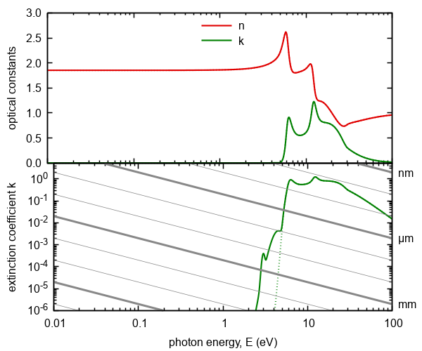
Figure 11. Optical constants calculated on the basis of the model included excitations between two types of localized states.
Doted lines represent model without these excitations. The gray lines represents absorption thresholds
for given thickness of ambient.
Free electrons contributions
It will be implemented.Core electrons excitations
It will be implemented.Phonon absorption
Phonon absorption is modeled in the UDM as Gaussian-broadened discrete spectra, similarly to absorption of the localized states.
The only difference in the parametrization is the use of different units for characteristic energy and broadening parameter:
modelfile
Universal:ex=2:he:ut:loc=2:ph=6
parfile
ex=2:he:ut:loc=2:ph=6
Nvc = 400
Eg = 5
Eh = 30
A0 = 1
Aex1 = 0.2
Eex1 = 6
Bex1 = 0.5
Aex2 = 0.3
Eex2 = 12
Bex2 = 1
Nvx = 1000
Ex = 10
Nut = 40
Eu = 0.1
Nloc1 = 0.1
Eloc1 = 4.5
Bloc1 = 0.5
Nloc2 = 0.001
Eloc2 = 3
Bloc2 = 0.1
Nph1 = 0.1
nuph1 = 1000
betaph1 = 100
Nph2 = 0.01
nuph2 = 750
betaph2 = 100
Nph3 = 0.05
nuph3 = 500
betaph3 = 100
Nph4 = 0.01
nuph4 = 1250
betaph4 = 100
Nph5 = 1e-5
nuph5 = 3600
betaph5 = 100
Nph6 = 1e-4
nuph6 = 100
betaph6 = 2500
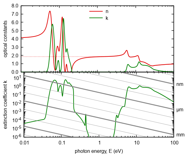
Figure 12. Optical constants calculated on the basis of the model included six phonon excitations.
Doted lines represent same model without these phonon excitations. The gray lines represents absorption thresholds
for given thickness of ambient.
We chose a model with six absorption peaks representing hypothetical material to demonstrate the phonon absorption. Narrow absorption peaks with well-defined wavenumber in this example represent single-phonon processes (first 5 absorption peaks). The first 4 represents the vibrations of majority atoms in atomic matrix. Wavenumbers of such vibrations are in the order of hundreds 1/cm up to approx. 1000 1/cm (heavier atoms have lower specific frequencies, lighter atoms have higher frequencies). The fifth absorption peak at thousands of 1/cm represents bond of light atom with the matrix of heavier atoms (the specific value of 3600 1/cm corresponds to the OH bond) The strength of this peak is proportional to the concentration of specific group (OH) in the material (this is valid only for low concentrations). The last peak can not be connected to single-phonon absorption. It represents a broad band corresponding to multi-phonon processes. The number of peaks chosen in the dispersion models is material specific and also depends on the sample thickness While for thin film it is usually sufficient to model the strongest peaks of single-phonon absorption, it is needed for thick films (tablets) to model even weaker processes of multi-phonon absorption (in this case the efficiency of the model decreases with number of absorption peaks).
Published
| Material | Form | Sample | Characterization | Range | Published | Produced | Submitted | Download |
| Al2O3, alumina, aluminium oxide | amorphous film (120 nm) | X2890 | ellipsometry & photometry | FIR (80 1/cm) - VUV (10.8 eV) | SPIE 9628 (2015) 96281U | Meopta | Daniel Franta | parfile table figure |
| Si, silicon | crystalline, Float zone | ellipsometry & photometry | FIR (80 1/cm) - VUV (8.5 eV) | unpublished | Daniel Franta | parfile table figure | ||
| HfO2, hafnia, hafnium dioxide | amorphous film (120 nm) | X2194 | ellipsometry & photometry | FIR (80 1/cm) - VUV (10.8 eV) | Applied Optics 54 (2015) 9108, SPIE 9628 (2015) 96281U | Meopta | Daniel Franta | parfile table figure |
| SiO2, silica, silicon dioxide | amorphous slab (0.405 mm) | Lithosil Q2 | ellipsometry & photometry & OC (Palik data & Schott prism) | FIR (80 1/cm) - VUV (8.5 eV) | SPIE 9890 (2016) 989014 | Schott | Daniel Franta | parfile table figure |
| MgF2, magnesium fluoride | polycrystalline film (120 nm) | X2935 | ellipsometry & photometry | FIR (80 1/cm) - EUV (50 eV) | SPIE 9628 (2015) 96281U | Meopta | Daniel Franta | parfile table figure |
| SiO2, silica, silicon dioxide | amorphous film (800 nm) | X2546 | ellipsometry & photometry | FIR (80 1/cm) - EUV (45 eV) | SPIE 9890 (2016) 989014 | Meopta | Daniel Franta | parfile table figure |
| SiO2, silica, silicon dioxide | amorphous film (800 nm) | X2551 | ellipsometry & photometry | FIR (80 1/cm) - EUV (50 eV) | SPIE 9628 (2015) 96281U | Meopta | Daniel Franta | parfile table figure |
| SiO2, silica, silicon dioxide | amorphous film (800 nm) | X2551 | ellipsometry & photometry | FIR (80 1/cm) - EUV (45 eV) | SPIE 9890 (2016) 989014 | Meopta | Daniel Franta | parfile table figure |
| Ta2O5, tantalum pentoxide | amorphous film (200 nm) | X2656 | ellipsometry & photometry | FIR (80 1/cm) - VUV (8.7 eV) | SPIE 9628 (2015) 96281U | Meopta | Daniel Franta | parfile table figure |
| TiO2, titania, titanium dioxid | amorphous film (100 nm) | X2801 | ellipsometry & photometry | FIR (80 1/cm) - VUV (10.8 eV) | SPIE 9628 (2015) 96281U | Meopta | Daniel Franta | parfile table figure |